Even though the graphics cards market has been moving quite a lot in the recent year 2016, especially since September until now, with the launch of the new Polaris 10 and 11 graphic cores by AMD Radeon, and the Pascal cores by NVIDIA, the market continues to exploit basically a similar architecture. This is something Radeon Group plans to change with the upcoming Vega graphics cards, which will implement new components within the core that will make them the most powerful and efficient models that AMD has manufactured to date.
The first thing I want to say is that in this article I am only going to talk about the new architecture, given that the graphics cards themselves are scheduled to launch in the first HALF of 2017, So do not expect photos of the graphics cards, given that there are still 3 to 5 months left for these kinds of photos to be released. Anyway, while Polaris 10 and 11 were the last efforts by the AMD to regain ground in the mid-range, I assure you that Vega is 100% designed to be a high-end graphics card.
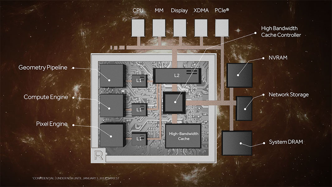
That said, I will start with a first image of what will be Vega’s internal schematic architecture:
Perhaps, the most important thing that Vega brings to the board right now is its new computing architecture called NCU (Next Generation Compute Unit), which is capable of handling two FP16 floating point instructions within a single FP32 instruction.
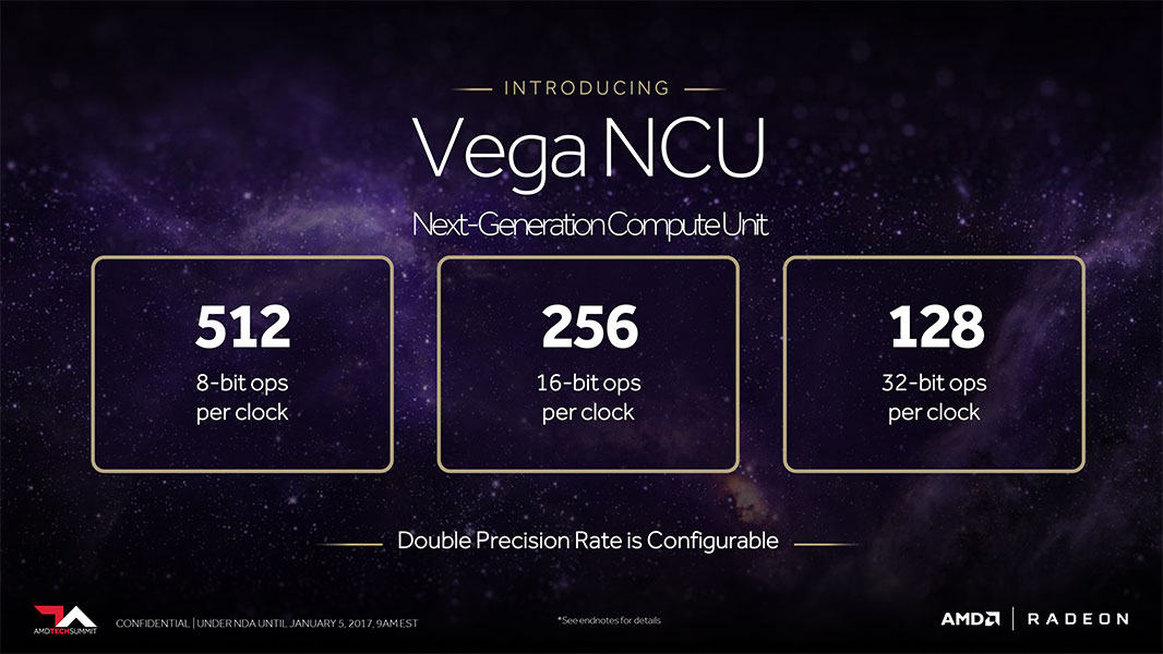
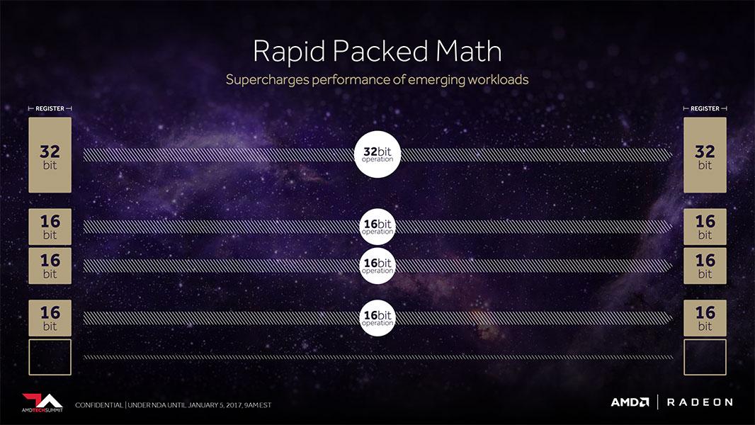
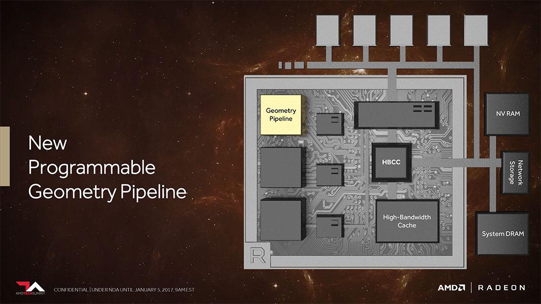
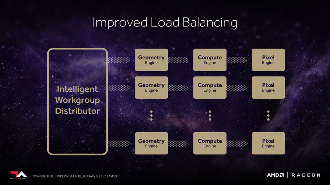
Another area in which Vega is going to be interesting is in his introduction of a new line of programmable geometry, capable of giving up to twice the number of operations per clock cycle, given that this new architecture is designed to handle up to 11 polygons per each clock cycle, using 4 geometry motors.
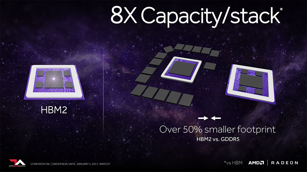
Of course, another one of the big things of these new graphics is the use of the new HBM2 graphic memory, which evolved from HBM that was already used with the launch of Radeon R9 Fury graphics. In this case, the new memories will no longer be virtually hidden to the poor 4 GB of the original HBM, but it will be possible to create graphics with up to 32 GB of video memory. Although, this could only be useful in the graphics market for workstations. However, another major improvement has been to double the bandwidth available for each pin, which would, of course, eliminate the current bottleneck that the HMB memory presents.
And so far, that is everything that AMD Radeon has wanted to share with us even though, tremendously interested in the possibilities of awakening, it is still quite little and leaves in sight more unknown prospects than what it reveals. But, of course, in ULITE, we will continue to inform you of everything that AMD Radeon wants to show us regarding the future.
Read More:
Best Budget Graphics Cards 2017 Between 200 and 400 dollars